








Collaboration aims to accelerate development of the manufacturing and design capabilities needed for future nanostack generations
By IBM Corporation
Today, IBM, in collaboration with Siemens, announced new research aimed at advancing IBM’s nanostack architecture, a new transistor architecture unveiled by IBM earlier this year. The collaboration will bring together IBM's leadership in semiconductor device innovation and Siemens' expertise in electronic design automation (EDA), process simulation, lithography optimization, and advanced manufacturing software to accelerate the development of nanostack.
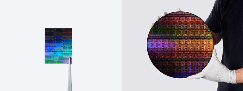
Nanostack is the industry’s first known three-dimensional, nanosheet-based design, vertically stacking and staggering transistors to pack more transistors onto a chip, with nearly 100 billion transistors in a space the size of a fingernail at its current 7 angstrom node. The design also unlocks the use of different material combinations within each stacked layer to optimize performance and power efficiency of each transistor independent of the other. These innovations power substantial leaps in energy efficiency, performance, and SRAM scaling.
Earlier this year, IBM demonstrated the viability of the nanostack architecture. Now, additional advances are needed to prepare the technology for manufacturing and production at scale.
Through this collaboration, IBM and Siemens will work to advance the design, simulation, and lithography techniques needed for this and future nanostack generations beyond the current 7 angstrom node. The collaboration includes developing advanced virtual models of nanostack in order to model performance, optimize designs, and address fabrication challenges before chips are built.
"Nanostack is a scalable transistor platform designed to shift device scaling from 2D to 3D, representing a new paradigm for the semiconductor industry and a path forward for the logic scaling needed to support AI and other emerging technologies over the coming decade,” said Huiming Bu, Vice President of Silicon Technology R&D, IBM. “We are thrilled to work with Siemens as we continue to advance this technology and explore new approaches to extend angstrom-level scaling with nanostack.”
“Scaling semiconductors into the angstrom era demands tightly coupled co-optimization between device physics, EDA design and manufacturing software, and manufacturing. As physical AI places extraordinary demands on silicon architecture, IBM’s 3D nanostack design represents a pivotal leap forward,” said Ankur Gupta, Executive Vice President, EDA IC Portfolio, Siemens. “Siemens’ collaboration with IBM to advance virtual modeling, simulation, lithography, and design software optimizations needed to address physical limitations early and accelerate the development of these complex architectures is truly pioneering.”
By combining IBM's semiconductor leadership with Siemens' advanced EDA software and simulation technologies, the companies aim to accelerate technology development cycles and advance the manufacturing foundation necessary for bringing nanostack toward production.
 Business users want new applications now. Market and regulatory pressures require faster application updates and delivery into production. Your IBM i developers may be approaching retirement, and you see no sure way to fill their positions with experienced developers. In addition, you may be caught between maintaining your existing applications and the uncertainty of moving to something new.
 IT managers hoping to find new IBM i talent are discovering that the pool of experienced RPG programmers and operators or administrators with intimate knowledge of the operating system and the applications that run on it is small. This begs the question: How will you manage the platform that supports such a big part of your business? This guide offers strategies and software suggestions to help you plan IT staffing and resources and smooth the transition after your AS/400 talent retires. Read on to learn:
LATEST COMMENTS
MC Press Online