








Built with revolutionary “nanostack” 3D chip architecture, IBM’s sub-1 nm chip to propel semiconductor industry forward for the next decade
By IBM Corporation
IBM today unveiled a major semiconductor breakthrough with the introduction of the world’s first sub-1 nanometer (nm) chip technology, featuring a revolutionary transistor architecture at the 0.7 nm, or 7 angstrom node. The achievement marks a landmark moment for an industry facing the physical limits of traditional chip scaling. Semiconductors play critical roles in everything from computing, to appliances, to communication devices, transportation systems, and critical infrastructure.
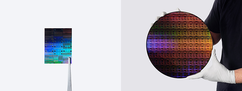
IBM’s new sub-1 nm chip packs nearly 100 billion transistors onto a chip the size of a fingernail, nearly twice the density of IBM’s 2 nm chip, unveiled in 2021. Enabled by a series of structural and material innovations, including IBM’s groundbreaking three-dimensional nanostack architecture, the technology demonstrates how continued gains in performance and efficiency remain possible even as chip features approach atomic dimensions.
Published technical results report the new chip is projected to offer a substantial leap in capability—up to 50 percent more performance, or 70 percent greater energy efficiency than IBM’s 2 nm node chips[1]—supercharging compute for applications ranging from generative AI and cloud infrastructure to next-generation electronic devices.
IBM’s latest chip breakthrough marks a landmark moment in computing, pushing technology beyond the nanometer era to the scale of atoms. With our new nanostack architecture, we’re not just making smaller transistors, we’re reinventing how chips are built to deliver dramatically more power and energy efficiency,” said Jay Gambetta, Director of IBM Research and IBM Fellow. “This industry-first innovation continues IBM’s legacy of leading in next-generation technologies and sets the foundation for the next era of computing.
Nanostack, an Industry Breakthrough in Chip Design
To produce this chip, IBM researchers developed an entirely new transistor architecture, called “nanostack,” the industry’s first known three-dimensional, nanosheet-based design. Nanostack represents a major advance beyond nanosheet technology, the industry’s current leading-edge architecture, invented by IBM. The nanostack design vertically stacks and staggers transistors, taking advantage of 3D sequential integration to pack more transistors onto a chip. The design also unlocks the use of different material combinations within each stacked layer, optimizing performance and power efficiency of each transistor independent of the other.
IBM’s nanostack architecture was experimentally validated through ultra-thin dielectric bonding in CMOS integration, demonstration of dual-channel engineering capability, and functional CMOS inverter operation with expected switching performance. Together, these results confirm the nanostack technology can be physically built and supports real computation.
Additionally, in new research presented at VLSI 2026, IBM researchers demonstrated that the nanostack architecture provides 40 percent scaling in SRAM,[2] unlocking the ability of chip designers to create much more efficient chips while also supporting the high-bandwidth data demands of advanced AI workloads.
With this groundbreaking structure, logic technology can extend for the first time below the 1 nm node, advancing the era of angstrom-level scaling, where dimensions approach the size of individual atoms. While transistor nodes now refer to a generation of manufacturing technology versus an exact physical dimension, IBM’s 0.7 nm technology—also referred to as 7 angstroms—demonstrates how continued scaling remains possible. With the new nanostack architecture, IBM’s semiconductor roadmap projects at least a decade of future scaling.
Building on Decades of Leadership in Semiconductor Innovation
This breakthrough is the latest testament to IBM as a leader in semiconductor R&D. IBM has led the world in developing the chips that power computing systems for decades, from early semiconductors in the 1960s to the world’s first 2 nm node chip. IBM continues to innovate at the cutting edge of silicon, AI hardware, logic, and quantum processors developed to power the future of computing.
IBM and its partners conduct this work at a leading semiconductor research facility in Albany, New York, which will soon be home to a High Numerical Aperture Extreme Ultraviolet (High NA EUV) lithography tool, essential for the future of logic scaling. Developed by ASML, this technology enables ultra‑precise circuit printing, supporting the creation of smaller, more powerful chips. IBM and partners including Lam Research Corp. (Nasdaq: LRCX), Tokyo Electron (TEL), and SCREEN Semiconductor Solutions, Ltd. have been working together to develop new High NA EUV processes and tools that have already yielded working devices.
IBM also recently announced a plan to form Anderon, the world’s first pure-play quantum foundry. Anderon, a standalone IBM company, will draw on IBM’s industry-leading quantum computing and semiconductor expertise to help position the United States to manufacture most of the world’s quantum wafers.
With the expectation of the earliest adoption of nanostack technology at the sub-1 nm node, IBM sees a path to production in as early as the next 5 years.
 Business users want new applications now. Market and regulatory pressures require faster application updates and delivery into production. Your IBM i developers may be approaching retirement, and you see no sure way to fill their positions with experienced developers. In addition, you may be caught between maintaining your existing applications and the uncertainty of moving to something new.
 IT managers hoping to find new IBM i talent are discovering that the pool of experienced RPG programmers and operators or administrators with intimate knowledge of the operating system and the applications that run on it is small. This begs the question: How will you manage the platform that supports such a big part of your business? This guide offers strategies and software suggestions to help you plan IT staffing and resources and smooth the transition after your AS/400 talent retires. Read on to learn:
LATEST COMMENTS
MC Press Online